
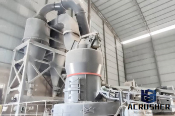
chemical etching process for sem manufacturer Grasping strong production capability, advanced research strength and excellent service, Shanghai chemical etching process for sem supplier create the value and bring values to all of customers.
 WhatsApp)
This etching is a wetbased process that increases the ... (SEM) images of Si ... Nonlinear Etch Rate of AuAssisted Chemical Etching of Silicon ...
Wet and Dry Etching ... chemical etching, ... A wet etching process involves multiple chemical reactions that consume the original reactants
Effects of the Nitric Acid Concentrations on the Etching Process, ... of porous zinc oxide by wet chemical etching. ... etching time, as discussed in SEM ...
Chemical Etching of Natural Fluorapatite Crystals in Acid Solutions Studied ... Different aspects of the chemical etching process ... chemical etching, fluorapatite, SEM
This sequence of patterning and etching is repeated multiple times during the chip making process. Etch processes ... physical and chemical etching such ...
A 3D Simulator for Silicon Anisotropic Wet Chemical Etching Process ... anisotropic etching process simulation ... chemical etching of crystalline ...
How to Acid Etch Steel. ... sulfate from coating the steel with a deposit of copper that will stop the etching process. ... The etching chemical, ...
Dummy Poly Silicon Gate Removal by Wet Chemical Etching T ... for the dummy poly silicon gate removal process, ... that the TMAH wet chemical etching is a ...
Chemical Etching (aka Photochemical Machining, ... Close up SEM image of partial ... For suspensions our photochemical etching process is capable of producing 1 mil ...

Chemical Etching and Patterning of Copper, Silver, ... etching. The chemical process ... which is consistent with preliminary SEM results. 100. Analogous to Cu ...
WetChemical Etching and Cleaning of Silicon ... following is a typical RCA process; ... with all wetchemical etching solutions, ...
Etching is used in microfabrication to chemically remove layers from the surface of a wafer during manufacturing. Etching is a critically important process ... SEM ...
The first of the two etching steps in the crystallographic etching process is used to ... SEM images of the two etch ... Crystallographic Wet Chemical Etching of p ...
Electronassisted chemical etching of ... alterations that occur during electronassisted chemical etching of ... chemical etching process, ...
To solve the problems generally encountered during the plasma electrolytic oxidation (PEO) of Al alloys with high Si content, a pretreatment of chemical etching was ...
complementary chemical etching process, ... SEM images of an electrical discharge machined titanium microelectrode array that has undergone the chemical etching ...
Controllable fabrication of fiber nanotips by dynamic chemical etching based on siphon principle ... chemical etching process.
... assisted chemical etching process in ... chemical etching process on lithographically ... lithographically defined areas formation kinetics ...
Metalassisted chemical etching of CIGS thin films for grain ... wet chemical etching process to define CIGS ... can make the etching difference observable under SEM.
... dissolution of agarose stamp into hot water demonstrates an environmentally friendly method by the moldassisted chemical etching process ... SEM images of ...
... we have developed a novel method for Pt etching using a chemical dry etching ... under various etching conditions. Chemical analysis of ... SEM studies of the Pt ...
The Preparation of Silicon Nanowires Using MetalAssisted ... Silicon Nanowires Using MetalAssisted Chemical ... Chemical Etching, Silicon Nanowires, SEM.
... does not possess the ability to etch BST thin films annealed at high temperature, ... microscope (SEM) ... during the wet chemical etching process due to ...
fabricate AlN (Aluminum Nitride) piezoelectric microstructures for actuator applications. ... the AlN thin film during the sacial etching process ... (SEM). The ...
WhatsApp)